Authors: John Lee and Puneet Gupta
https://doi.org/10.1561/1000000019
Preliminaries
At the very start of the physical design process is logic synthesis. The goal of logic synthesis is to transform a Register Transfer Language (RTL) design description into a gate level netlist. Gate cells either comprise of Boolean logic functions, such as NAND and XOR, or as sequential cells such as a flip-flop which provides memory to the design. The ISPD 2012 benchmarks provide one flip-flop and 11 Boolean logic functions each having 3 different voltage thresholds and each voltage threshold has 10 different sizes.
Logic gates are designed to input and output either a “high” or “low” voltage representing 1 and 0 respectively. In an ideal world, the voltages would only exist at these extreme limits. However, this is not the case in reality. Thus, each gate has a corresponding voltage threshold which is used to distinguish between a “high” and “low” voltage.
Consider a simple inverter gate:
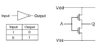
It is comprised of two transistors:
- A PMOS transistor connected to power supply
- A NMOS transistor connected to ground
When is high, the NMOS transistor turns on directing the flow of electricity to ground, hence is low. When is low, the PMOS transistor turns on allowing the flow of electricity from towards , hence is high. Increasing the size of these transistors increases the current which reduces delay. However, by increasing the transistor size, the required load to drive the gate increases.
Each choice of gate sizing and voltage threshold has an effect on the following metrics:
- Dynamic power - power consumed every time a gate switches
- Leakage power - subthreshold current bleeding through “off” transistors
- Clock period - time to complete a single cycle
The goal of gate-sizing is to select the sizes of gates from a library which minimize power while avoiding too high of a delay. That is, if we let be a vector of cell options, then we get the optimization problem
where is the clock period. Since the choices of gate sizes come from a predefined library, we have integer constraints on .
Static Timing Analysis
The goal of Static Timing Analysis (STA) is to determine the delays and arrival times in the graph without inputs or simulation, whereas dynamic timing methods require simulation. The guiding principle of STA is propagate the best- and worst-case delays through the circuit. Each node is given an arrival time, , which are computed by traversing the circuit: start with the primary inputs, and propagate the delays through towards the outputs. Slacks, , on the other hand are computed in reverse: start with the required arrival time at each output and propagate backwards.
Concepts and Terminology:
- Primary inputs: input ports in the design that are driven by external sources
- Primary outputs: output ports in the design
- Fanins of a gate (): set of gates that drive the inputs of gate
- Fanouts of a gate (): set of gates that are driven by gate
- Fanin cone of a gate: set of gates whose outputs have a path to the input of the given gate
- Fanout cone of a gate: set of gates whose inputs have a path from the output of a given gate
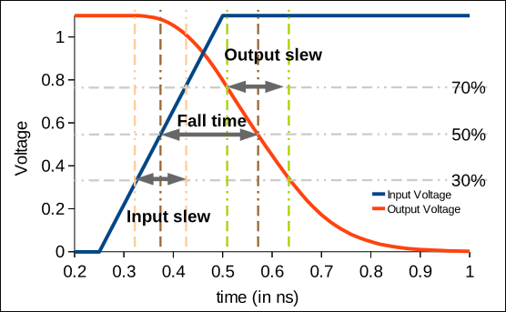
- Rise delay: time from when the input crosses voltage to when the rising output crosses voltage
- Rise transition/slew: time from when the output crosses voltage to when it crosses voltage
- Arrival time (): the time that the signal crosses the voltage threshold at a given point in the circuit
- Required arrival time (): the time a signal needs to cross the voltage threshold at a given point in the circuit
- Slack ():
A timing is infeasible if there is a negative slack, , and feasible if all slack are non-negative, . In other words, a timing is feasible if all signals arrive on or before the required time.
Computing Arrival Times and Slacks:
- Compute the delays and arrivals times at the primary inputs and the flip-flop outputs.
- In topological order, compute the delays and arrival times for the remainder of the gates.
- Compute the arrival times at the primary outputs and the flip-flop inputs.
- In reverse-topological order, compute the required arrival times and slacks.
In the above, topological order corresponds to numbering the gates through a graph traversal such as BFS or DFS.
Question: Is the graph always acyclic?
Some sources include interconnect delays by computing the delay from wires. In order to get the most accurate interconnect delay requires one to solve a system of differential equations relating current, charge and voltage. However, this is computationally expensive so many incorporate a first-order approximation known as the Elmore delay which provides an upper bound on the actual delay.
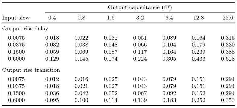
The delay from cells is often stored in the Synopsys Liberty modeling format which typically makes use of the Nonlinear Delay Model (NLDM) which is comprised of tables storing the rise and fall times and output rise and fall transitions (slew) as a function of the input transition and output capacitance load. For instance, the table below gives the rise times (delays) and transitions (slews) in nanoseconds for a given inverter gate:
Instead of rise delay and rise transition, flip-flops report setup time and hold time.
The load capacitance is typically not well-defined at the output of a gate. STA timers typically accommodate for this by computing the effective capacitance of a gate.
Computing Power:
All Liberty models also provide leakage power information for a given cell. For instance, the 45 nm Nangate Library gives the following information for the NAND2_X1 gate:
| Leakage Power | ||
|---|---|---|
| 0 | 0 | 1017.82 |
| 0 | 1 | 7340.61 |
| 1 | 0 | 1204.57 |
| 1 | 1 | 10286.09 |
Similar to the Nonlinear Delay Model (NLDM), the Liberty model uses a Nonlinear Power Model (NLPM) which provides a series of tables for the rise and fall of power of the cell, as a function of the input transition and output load.
Gate Sizing
Delay is roughly related to gate size, length and by the power law
where is the gate-to-source voltage. The specifics of the relation between gate size and delay depends heavily on the gate technology.
The dynamic power of a gate depends on the total capacitance, , and the frequency of gate switches, :
The capacitance, , is linearly related to the area of the gate. A smaller aspect to dynamic power is short-circuit power. During the brief period where the PMOS and NMOS transistors are in transition, some power is lost. This power loss can be minimized by accelerating the input transition time.
There are several sources of leakage power, with the main source being due to a transistor never being fully “off”. The leakage power is related linearly to gate-width, but exponentially to threshold voltage . The leakage power also depends on the current input of the gate (see table above for NAND2_X1 gate).
Example:
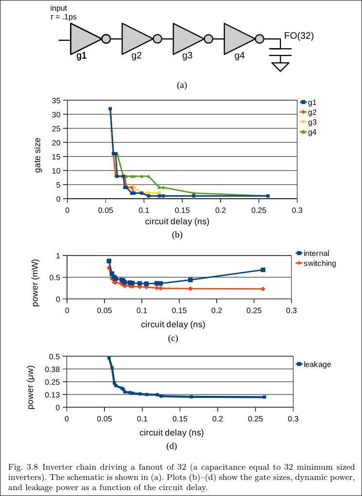
Methods for Discrete Gate Sizing and Assignment
Denote as follows:
- - Set of gates in the design
- - A gate in the design
- - A cell option, current cell option
- - Set of alternative library cell options for
- - The width for gate
- - The threshold voltage for gate
- - Arrival time
- - Set of arrival times for the inputs of gate
- - Required arrival time
- - Set of required arrival times for the inputs of gate
- - Set of input transition slews for gate
- - Delay
- - Power
- - Primary inputs
- - Primary outputs
- - The set of gates that drive the inputs of gate
- - The set of gates that are connected to the output of gate
Linear Programming Based Assignment Method:
We approximate the power of a design by
where is the width of gate and is the power of gate . Unfortunately, the gate delay is not linear. We approximate with the following linearization
where are coefficients, and is the input capacitance of gate . Our constraint places bounds on the arrival times of gates:
We also need to capture the order of arrival in gates. That is, if then the signal arrives to before . More precisely,
Putting this all together results in the following linear program:
References:
- J. Fishburn, A. Dunlop. “TILOS: A posynomial programming approach to transistor sizing.”
- Y. Tamiya, Y. Matsunaga. “LP based Cell Selection with Constraints of Timing, Area, and Power Consumption.”
Integer Linear Programming Based Assignment Method:
The above model chooses gate sizes, , continuously. In typical cases, such as ISPD2012, the available gate sizes are discrete. One may round to the nearest available gate size. However, a more accurate approach is to model the problem using integer constraints.
Define the assignment variable
We assume we currently have an assignment of gates to cells. Then the objective is to minimize
where
is the change in power of our new assignment from to . We also change the computation of delay so that
where is the change in delay if we change the gate from to .
In summary:
The authors of this approach relax the binary constraints by treating as continuous between 0 and 1 and use as a threshold value. However, relaxing the constraints may result in timing violations.
References: