Authors: Chung-Ping Chen, C.C.N. Chu, D.F. Wong
Link to full paper: https://ieeexplore.ieee.org/document/743080
Preliminaries
Define
- to be the driver resistance for the th input driver, .
- to be the load capacitance of the th output load, .
A gate, wire segment or an input driver is referred to as a component. We add two factitious components to our circuit:
- An output component which consists of all output loads.
- An input component which consists of all input drivers. We refer to the connection point two components as a node. We also treat the output point of our output component as a node. There are components and nodes, where is the number of gates or wire segments.
Label the nodes , where , in reverse topological order. That is, index 0 is the output point of the output component and index for is the node connecting to the th output load. For , the node with index is the connection among the gates and wire segments. By this ordering, if node is connected to the input and node is connected to the output, then . We also index the components if the output is connected to node .
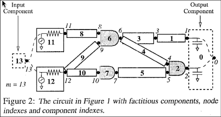
Define
- to be the set of indexes of components directly connected to the input(s) of component .
- to be the set of indexes of components directly connected to the output of component .
- to be the set of indexes of gates
- to be the set of indexes of wire segments
- to be the set of indexes of input drivers
- For , let be the gate size, the output resistance, and the input capacitance of the pin (we assume all pins share the same input capacitance).
- For , let and be the unit size output resistance and input capacitance per unit size of gate , i.e., and .
- For , is the segment width.
- For , let , and be the unit width wire resistance, the wire area capacitance per unit width and the wire fringing capacitance of segment . Then for wire , and .
- For , define and such that .
Components are modeled as RC circuits. This allows the use of Elmore delay model for delay calculation. Elmore delay along a signal path is calculated as the sum of the delays associated with the resistors in the path. Each component (exluding the two facitious components) is assumed to contain a resistor . For input driver , we define , i.e., the driver resistance of the th input driver (the is to get it in the right index. Recall is in . Each is offset by indices due to the labeling. Basically we are setting the resistance to that input drivers resistance.)
Let be the downstream capacitance of resistor . In short, the downstream capacitance of a resistor is given by the total capacitance of everything “downstream” resistor . For instance, in the figure below the downstream of capacitance of is as capacitors and are downstream of . But the downstream capacitance of is just .
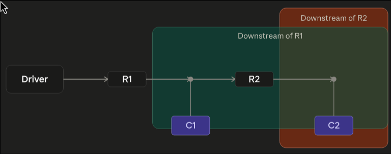
The Elmore delay associated with resistor is calculated by . Thus, if a signal path passes through resistors , then the Elmore delay along is given by
We denote the set of all possible paths from node to node 0 by , i.e., any is a path from an input driver to an output load.
Minimizing Total Area Subject to Maximum Delay Bound
Define to be the maximum delay form any input driver to any output load, i.e., is a bound on the arrival time at node . We wish to minimize the total component area, which can be computed by where are some constants. Thus, the problem is
However, there are exponentially many paths. So they partition the path delay constraints into constraints on component delay to form the primal problem:
The constraints for are as follows:
- Every input of our factious output component arrives no later than
- The arrival time of component cannot be earlier than its inputs with delay from component : .
- The arrival time of our input drivers is no less than the input driver’s delay
- Size constraints for components.
They relax constraints 1-3 to get the Lagrangian relaxation
where
Notice that the Lagrangian has two variables: component sizes and arrival times .
They use Kuhn-Tucker conditions to show that in order for the optimal solution, , for to also be the optimal solution for one needs for all (to ensure is a saddle point). That is, where
This results in a simpler problem which eliminates variables :
where
and
Lemma 1
For any , the optimal for is the same as the optimal for .
This leaves the following solving strategy:
- Solve to find the optimal
- Find the optimal by setting to be the smallest possible value that satisfies the constraints of .
Solving
Define
- to be the set of resistor indexes (excluding ) on the path(s) from component to the nearest upstream gate(s) or input driver(s). For instance, in Figure 2 above: .
- , i.e., the weighted upstream resistance of component .
- Modified downstream capacitance:
The phrase local re-sizing of component refers to changing while keeping the sizes of all other components fixed. The optimal local resizing of component minimizes .
Lemma 2
Let be a component-sizing solution. An optimal local re-sizing of component is given by changing the size of component to where and .
No proof for Lemma 2 is provided. Expression is found by minimizing while only changing component .
Their algorithm is a greedy algorithm that iteratively re-sizes each component. In each iteration, each component is examined in order and re-sized optimally using Lemma 2 while keeping the other components fixed. The algorithm then recomputes and incrementally by traversing the circuit in reverse topological order followed by topological order.
Algorithm 12
for do
end for
// Compute for by traversing the circuit in reverse topological order
for do
end for
for do
for all s.t. do
end for
end for
// Compute and for by traversing the circuit in a topological order
for do
for all do
end for
end for
If there was an improvement, goto line 5
The main aspect of the algorithm is on line 20 when we apply Lemma 2 to component . Lines 5-13 are simply walking along the circuit from right-to-left and keeping track of the downstream capacitance. Lines 16-19 are simply summing up the resistance from each input to the component. The component sizes and resistances are computed left-to-right.
The algorithm runs in time using memory, where is the number of sizable components and is the number of iterations.
Theorem 1
For any fixed vector , algorithm always converges to the optimal component-sizing solution of the problem
Again they claim this with no proof.
Solving the Lagrangian Dual
Define
They consider the Lagrangian dual problem:
They use subgradient optimization method to solve . See Lagrangian Relaxation for more details. In summary, the algorithm works as follows:
- Iteration 0: Start from an arbitrary
- Step :
- Solve (by solving ).
- For each relaxed constraint , compute the subgradient . For instance, for constraint the subgradient is where is the value given by our current solution .
- Set , where and is some step size.
- Project to the nearest point in .
They don’t specify the step size, the simplest would be . The only real requirement for convergence is that and .
Algorithm 13
,
while do
where
Solve via and then calculating
for do
for all do
end for
end for
Project onto nearest point in
end while