Authors: Ankur Sharma, David Chinnery, Tiago Reimann, Sarvesh Bhardwaj, Chris Chu
Link to paper: https://dl.acm.org/doi/abs/10.1109/TCAD.2019.2915324
Define
- = Target clock period
- = Set of gates in the design
- = Discrete set of cells for gate
- = Current cell assigned to gate
- = Leakage power of cell
- = Maximum load capacity of cell
- = Set of nodes in the timing graph
- = Set of input pins of gates and output ports
- = Set of output pins of gates and input ports
- = Set of timing endpoints, i.e., data input pin of a sequential gate or an output port
- Set of timing arcs in the timing graph
- = Arrival time at node
- = Gate or port associated with node
- = Lagrangian multiplier for the timing arc
- = Set of variables , and , e.g.,
- Delay of the timing arc from node to node
- = Slew at node
- = Effective capacitance at node
- = Maximum slew defined in the cell library
They use a similar primal problem as Fast and Exact Simultaneous Gate and Wire Sizing by Lagrangian Relaxation with the exception of the objective being to minimize leakage power instead of size:
Timing violations is quantified by total negative slack:
Then again like Chen et al., they take the Lagrangian relaxation of the primal:
Note that they do not relax the load and slew constraints; they claim these are easy to track. This leaves the first problem:
By Karush-Kuhn-Tucker optimality we get the following ideal values:
These are the same conditions as Chen et al., just with different notation. They refer to them as the flow constraints.
Remark: According to Wang et al., the KKT conditions are sufficient but not necessary.
The use to simplify into a new problem without the arrival times:
for . The sum is referred to as the lambda-delay sum. The objective of is called the LRS cost and it’s optimal value is denoted by .
Thus, the Langrangian Dual problem is given by
Remark: The term is from converting the optimal of back into by setting to the smallest possible value that satisfies , i.e., for all and for all . From this assumption, we get
Flow of the Algorithm
They make use of a five stage flow:
- Initialization
- Calibration of effective capacity
- LDP Solver for LR timing (solve )
- Calibration
- Greedy post-pass for greedy timing
The two calibration stages are done by passing the model to an external timer.
Initialization
- Set each gate to the size with the minimal leakage power
- Fix the maximum load and maximum slew violations.
- Scan design in reverse topological order, increase the size of gates that exceed the gate’s maximum load capacity.
- Scan design in forward topological order, increase the drive strength of any cells whose output slew is too high.
Calibration
Pass the current model to an external timer (Synopsys PrimeTime) and update our parameters. In the second stage, only the effective capacitance of each gate is updated. In the fourth stage, all timing parameters (including effective capacitance) are updated.
LDP Solver
The is solved in two-substages:
- LR timing recovery
- LR power recovery
Each of these substages follow the same design, which is iterative until the desired parameter converges or a cap of 200 iterations is reached:
- At step :
- Solve to find optimal and
- Perform static timing analysis
- Update Lagrangian multipliers
Algorithm 10 Solve
Compute local negative slack around each gate
for each gate in forward topolical order do
current of
for each valid cell alternative do
if and then
end if
end for
Apply to and update timing locally
end for
The algorithm walks through the design greedily setting each gate’s cell to the one with the minimal cost that reduces the , where cost is given by the sum of the cell’s leakage and a rough approximation of the delay (scaled by ):
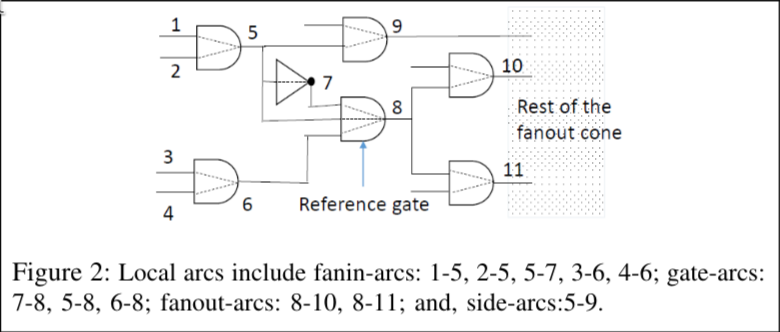
Here “local-arc” refers to fanin-arcs, gate-arcs, side-arcs and fanout-arcs in the area surrounding gate (see Figure below).
Timing Models and Calibration Mechanism
They use a “simple” RC model to estimate the effective capcitance as well as delays and slews for gates and interconnects. They’re RC model is calibrated in stages two and four with Synopsys Primetime.
Given a design, a net or interconnect is an RC tree composed of taps and wire segments connecting two adjacent taps. Each tap has a corresponding capacitance and a subtree rooted at . Wire segments connecting the parent of tap , , to to tap has a upstream resistance give by . The sum of all the resistances on the path connecting the root of the to tap is denoted by .
For estimating effective capacitance of a net , they use
where is a net-specific parameter and is the drive resistance (computed via lookup table) of the arc that drives net . By default , during calibration is updated so that matches the result from Synopsys PrimeTime. Before calibration, had an average error of , but a large standard deviation of and maximum error of .
They estimate slew by
where
- is the slew at the root of the net
- is the Elmore delay from the root of the RC tree to tap
- is the slew correction factor which initially is set to .
Elmore delay is given by the path from the root to tap :
where and are the upstream resistance and downstream capacitance at tap . They modify the Elmore delay by scaling it by a delay correction factor . is initially set to 1 and updated during calibration so that matches the result from PrimeTime.
Gate slew and gate delay are given by a lookup table then scaled by a slew correction factor and delay correction factor, respectively.
The calibration algorithm essentially boils down to three steps:
- Generate a verilog file for the design
- Run Synopsys PrimeTime
- Update various parameters so that our estimations match PrimeTime’s output
This is clearly the slowest part of their algorithm. On average, the calibration steps take of the runtime with a high of of the runtime.
Multi-Threaded LRS Solver
They speedup solving by using parallel computing. The idea is, that multiple gates can be sized simultaneously, but not any two gates can be resized at the same time.
In order for two or more gates to be resized simultaneously, they must satisfy two properties:
- None of them have a fan-in arc in common; and
- None of them lie in each other’s fan-out cone.
They first ensure property 1 is satisfied with an algorithm they call mutual exclusion edges (MEE):
Algorithm 11 MEE assignment
// Stage 1: Assign random IDs
for each level to maximum topological level do
for each gate in level do
while is not unique do
end while
if then
end if
end for
end for
// Stage 2: MEE assignment
for each gate in the design do
fan-outs of sorted by ascending IDs
for each to do
Assign MEE from to
end for
end for
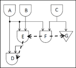
The MEE edges are essentially “dummy edges” to form a chain of fan-outs for every gate. For , they refer to as the pseudo fan-in of and as the pseudo fan-out of . An example is given in the Figure below; the dashed lines show the fanouts of () and () are connected by MEE edges. In this case, and cannot be resized simultaneously as they share a fan-in from . Likewise, and share a fan-in from . Finally and share a fan-in from . The MEEs enforce a sequential order for resizing fan-outs.
They ensure property 2 is satisfied with a DAG based netlist traversal:
- For each gate, let be the number of fan-ins and pseudo fan-ins of that gate that are yet to be resized.
- Initialize variable to total number of fan-ins and pseudo fan-ins.
- After a gate is resized, the variable for all its fan-outs and pseudo fan-outs is decremented by 1.
- Any gate whose is ready to be resized.