We can view a netlist as being comprised of several logic stages, where a logic stage refers to a component and the interconnect that it drives. For instance, a chain of four inverters would have four stages of combinational logic, one for each inverter. For digital circuits, each stage can be viewed independently and the delay along a path is simply the sum of the delays. Indeed, consider a netlist consisting of two inverter gates. There are three events in the timeline:
- : the input for stage 1 crosses voltage at time
- : the output for stage 1/input for stage 2 crosses voltage at time
- : the output for stage 2 crosses voltage at time
Then the total delay is given by
Gates taken from a library typically have their delay precharacterized by its load and input transition time , also called slew, and often presented by a look-up table. In the case of multi-input gates, the delay often assumes that only one input switches at a given time. This assumption is generally not accurate, and simultaneously switching inputs can significantly impact the delay.
Analysis of a Single Stage
One common problem in worst-case delay calculations for a gate, is determining the set of transistors that must be on. The most precise method to identify this set requires a full enumeration, which unfortunetly requires an exponential number of enumerations for transistors). A common heuristic is to make use of Elmore delay and a well-known graph problem. As an example, consider a CMOS gate which may be viewed as an undirected graph which has an edge between the drain and source nodes of each transistor and weighted by the resistance of the corresponding transistor (see below). We remove the node and its incident edges as the worse-case path will not involve this node. To determine the worst-case delay, the objective is to determine the set of edges that must be on to induce the largest Elmore delay for a switching event on transistor ; which results in a path, known as the largest resistive path, through from the output node to ground. Finding the LRP is equivalent to a longest path problem which is NP-complete. One may make it solvable in linear time by assigning directions to transistors, making our graph a directed acyclic graph.
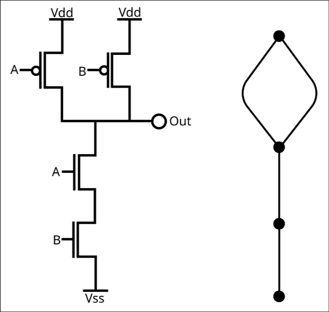
However, this approach may result in some transistors that need to be on in the worst-case but do not lie on the LRP. One may use the LRP to choose edges in the following order: walk along the LRP (starting at output node ) turning on transistors that maximize the downstream capacitance as you go.
Analysis of a Combinational Circuit
Given a combinational circuit, we construct a timing graph where the vertex set consists of the logic gates and the primary inputs and outputs of the circuit. Two vertices are connected by an edge if the output of is connected to the input of in the circuit. It is also often useful to add a single source node and single sink node , e.g., if the if all the primary inputs are connected to flip-flops and transition at the same time. Another useful transformation is in the case a primary input arrives at a different time than the other. Such a case can be handled by inserting a dummy node with delay along each edge from to .
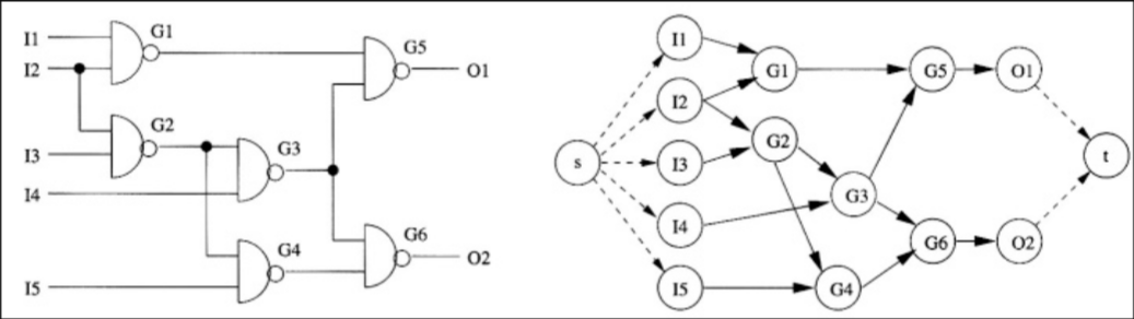
Because combionational circuits conventionally do not have cycles, our resulting graph forms a DAG. However, some implementations do allow for combinational circuits with cycles which an STA typically handles by breaking the cycles to form a DAG.
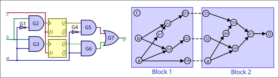
We can encode sequential circuits that consist of both combinational and sequential elements (flip-flops and latches) by a set of combinational blocks between latches and analyzing each block. The input of each block corresponds to the sequential elements or circuit inputs that fanout to a gate in the block; likewise, the sequential elements or circuit outputs for a which a fanin gate belongs to the block represents its primary outputs. Constructing these blocks is straightfoward: simply construct the combinational graph leaving sequential elements unrepresented. The connected components of this graph correspond to the combinational blocks in the circuit.
Delay Calculation for a Combinational Logic Block
The most popular method used in static timing analysis is called PERT (Program Evaluation and Review Technique), which is a misnomer as it more closely aligns with Critical Path Method (CPM) used in scheduling. In CPM, each gate is assigned two numbers corresponding to the output rising transition, , and the output fall transistion, . We assume all primary inputs are available at time zero, i.e., all primary inputs are assigned . The critical path method walks along the graph in topological order, computing the worst-case rise and fall arrival times at each intermediate node.
Algorithm 2 CriticalPathMethod
Initialize array indicating the number of times has been visited.
for all primary inputs do
for all vertices s.t. do
If , then add to .
end for
end for
while do
Compute the delay for gate
for all vertices s.t. do
If , then add to .
end for
end while
The algorithm is essentially a graph-traversal similar to DFS with the modification that a gate is only processed after all of its fanin gates have been processed as captured by the condition. Computing the delay is straight-forward, but depends on the type of gate. When processing a buffer gate all of its inputs have been processed, so we can simply take the maximum delay
where is gate’s output rsising transition and is the processed arrival rise time from gate . An identical formula is used for arrival fall time. An inverter gate on the otherhand, responds to the opposite signal, i.e., rises when the input is falling:
Upon traversing the entire graph, we are left with a two final arrival times . The worst-case delay is then taken as the maximum of the two: .
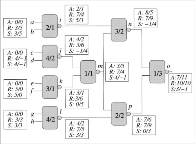
By assigning a required time to each node in our graph, we can capture two timing metrics:
- Arrival time at node
- Slack at node .
Typically only the required time is provided for the primary output. However with this information, one may find the required time for each node in the graph by performing CPM in reverse topological order.
We can also find the critical path which is defined as the path between an input and an output with the maximum delay, which can easily be found by backtracking after the critical path method. In the above figure this corresponds to . We can find this path using the arrival time: start at the primary output node and traverse the graph backwards choosing the input node with the worst maximum arrival time.
It is often the case that a small part only a small part of the circuit may be altered. In such a case, recomputing the entire STA results in a lot of unnecessary computation. For instance, if we alter gate in the above example, then its effect only propagates to the gates and and the arrival times of other gates are left unaltered. As a result, it is cheaper to only reprocess the gates whose arrival time may have changed. This incremental approach is called event-driven propagation.
The critical path method for finding the delay can be completed in time; which is a huge improvement over enumerating over all possible primary inputs. However, CPM makes the assumption that the actual logic function implemented is inconsequential to its delay. In otherwords, CPM pessimistically assumes that the critical path gives the circuits worst-case delay when there may be no set of inputs that excites said path. This is known as a false path. Many apporaches to false path analysis have been proposed, but are often too complex to be used in practice. See the survey Integrating Functional and Temporal Domains in Logic Design by Patrick McGeer and Robert Brayton.