Many tools, including Synopsys PrimeTime, model transistors by RC circuits. An RC circuit (or resistor-capacitor circuit) is a model of electric circuits composed of resistors and capacitors. For example, the Figure below is an example of a NOT gate. The actual RC circuit depends on the implementation of the gate, as most gates have multiple ways of being constructed.
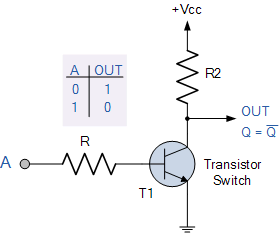
The diagram shows the VCC voltage (main power supply) connected to a ground through an NPN transistor which is controlled by an input line . When is high, the transistor closes connecting VCC to ground. At this stage we have the loop VCC → → → ground. Because of the resistor , this loop is dropping almost the entire supply voltage, leaving the OUT line to have nearly zero volts. When is low, the transistor is open, breaking our loop. As a result, little-to-no current flows through , allowing the voltage in the out line to rise.
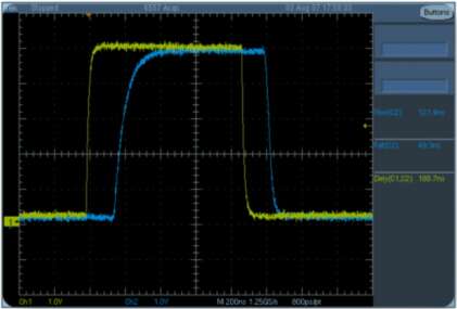
In an ideal world, a logic gate’s output signal would transition from low to high instantly. However, this is not the case in reality as the voltage takes time to rise. For instance, the figure below is a measure of the voltage of a buffer gate where the green/yellow trace indicates the input signal and the blue trace indicates the output signal. This figure shows that not only is there a propagation delay for the gate to respond to the input signal, but there is rise/fall times for the output signal.
More specifically:
- Propagation delay is the time between the input reaching 50% voltage and the output reaching 50% voltage.
- Rise time and Fall time is the time the output takes to transition between low-high states. Assuming a threshold of 10%, rise time corresponds to the time for the output to go from 10% to 90% voltage.
For simplicity, we assume that at all points in time.
Single Buffer Gate
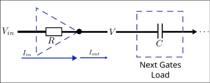
These timings are due to the gates resistance and capacitance . Consider the current flowing through a single buffer gate. An actual buffer gate is a bit complex, so we’ll simplify things and look at the following values of the buffer gate:
- Driving voltage is the voltage going into the buffer gate and is tied to the previous components output
- The gate has its own drive resistance
- The gates load is determined by the next gate’s input capacitance
- Output voltage .
We can view the buffer gate as a junction with one in current, , and one out current, . According to Kirchhoff’s current law,
The current coming out of the buffer gate is used to drive the input of the next gate(s) downstream. Logic gates are built from transistors, which are controlled by a control terminal (called a gate) used to control whether the source and drain are connected. Control terminals are a tiny sliver of conductive material separated from the rest of the transistor by an insulating layer. These two conductive layers separated by an insulator results in a capacitor (image). Thus, needs to charge the capacitor (technically the wire connecting the gates also has capacitance); which we can model using the current-voltage relationship:

The input current simply flows through the gate which has drive resistance . Ohm’s law states that the current between two points is directly proportional to the voltage across the two points. That is, the current through our buffer gate is simply
Thus, we get the linear differential equation
which captures the following RC circuit:
Solving this ODE gives us that
where is some unknown constant. Applying the initial condition and solving for gives us that
Thus, we can find the propagation delay by setting :
where is the RC time constant.
I compared our model to a SPICE simulation using and , which corresponds to a propagation delay of . Other than a slight error at the pulse edge, our model performs very well with an average error of and standard deviation of . The spike of error at the pulse edge is likely do to my code detecting when reaches 50% as transitions from to in .
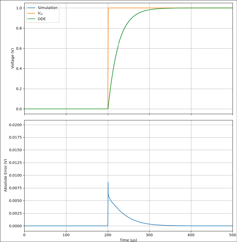
That being said, all this result essentially shows us is that our math is correct as SPICE simply converts the circuit into a system of differential equations and solves numerically. In fact, our model is probably more accurate.
Elmore Delay
Adding more gates into the circuit results in the differential equation becoming quite unwieldy. For that reason, many people choose to crudely approximate the RC time constant with Elmore delay. The idea behind Elmore delay is to compute the average of instead of computing itself. That is, the Elmore delay is given by
This integral can be solved from the circuits topology. At each node in the circuit, the Elmore delay is given by
where the sum is taken across the path from the source node to node . Here is the resistance of the path segment . Solving for where is the final node gives us
where the inner sum is the downstream capacitance.
Deriving Elmore Delay
Our RC circuit is a system that produces an output signal from any input signal , where is the Dirac delta function. If you provide two input signals and , then the output of the system is linear: ; or in simpler terms, doubling the input voltage doubles the output voltage. The system is also time invariant, meaning the output doesn’t change if we apply an input now or 5 seconds from now. This type of system is called a linear time-invariant system.
When the system is provided an impulse signal , it produces a response so that
Consider the impulse signal at time and . At each point in time, our output signal is given by and , respectively. Therefore, our response over this time frame is given by
Applying the fundamental theorem of calculus and letting gives us that .
Instead of working in the domain of time, we want to work in the frequency domain. Define our input signal , where is the complex-valued frequency. Then it follows that
i.e.,
where is the transfer function of our system. If we replace with a series, then becomes
Thus, taking the first two terms gives us
Notice that our approximation for is our input frequency delayed by , i.e.,
Therefore, a first-order approximation for the delay is .
Computing Elmore Delay
Returning back to our single gate model, we found that
According to the differentiation property of the Laplace transform, . Thus, if we take the Laplacian of our differential equation we get that
Thus, it follows that
This forms a power series, so
Taking the first-order approximation gives . However, we originally found that . Therefore, it follows that .
Extending beyond a single gate requires setting up a system of linear differential equations. For instance, if we have a chain of buffer gates in serial then we need to solve the following system:
Or in matrix form, where (defining ),
Taking the Laplace transform of each equation gives us:
Chaining them all together gives:
Thus, the final delay is given by
If we assume all buffer gates have the exact same resistance and capacitance, then the actual solution to our system (according to Claude) is
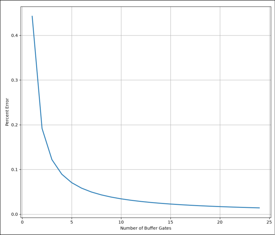
Using a fixed , I numerically approximated the delay given and the Elmore delay model for . Surprisingly, the Elmore delay performs quite well as the number of gates increase.